- 您现在的位置:买卖IC网 > Sheet目录337 > LH28F320S3HNS-ZM (Sharp Microelectronics)IC FLASH 32MBIT 110NS 56SSOP
LHF32KZM
9
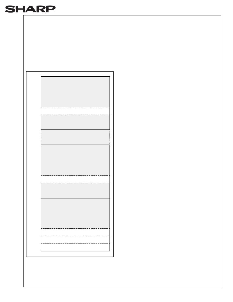
3.5 Read Identifier Codes Operation
The read identifier codes operation outputs the
manufacturer code, device code, block status codes
for each block (see Figure 4). Using the manufacturer
and device codes, the system CPU can automatically
match the device with its proper algorithms. The
block status codes identify locked or unlocked block
setting and erase completed or erase uncompleted
condition.
3FFFFF
Reserved for
Future Implementation
3F0006
3.6 Query Operation
The query operation outputs the query structure.
Query database is stored in the 48Byte ROM. Query
structure allows system software to gain critical
information for controlling the flash component.
Query structure are always presented on the lowest-
order data output (DQ 0 -DQ 7 ) only.
3.7 Write
Writing commands to the CUI enable reading of
device data and identifier codes. They also control
inspection and clearing of the status register. When
V CC =V CC1/2 and V PP =V PPH1/2/3 , the CUI additionally
controls block erase, full chip erase, (multi) word/byte
write and block lock-bit configuration.
The Block Erase command requires appropriate
3F0005
3F0004
Block 63 Status Code
command data and an address within the block to be
erased. The Word/byte Write command requires the
3F0003
3F0000
3EFFFF
Reserved for
Future Implementation
Block 63
command and address of the location to be written.
Set Block Lock-Bit command requires the command
and block address within the device (Block Lock) to
be locked. The Clear Block Lock-Bits command
020000
01FFFF
010006
(Blocks 2 through 62)
Reserved for
Future Implementation
requires the command and address within the device.
The CUI does not occupy an addressable memory
location. It is written when WE# and CE# are active.
The address and data needed to execute a command
are latched on the rising edge of WE# or CE#
(whichever goes high first). Standard microprocessor
write timings are used. Figures 19 and 20 illustrate
WE# and CE#-controlled write operations.
010005
010004
Block 1 Status Code
4 COMMAND DEFINITIONS
010003
010000
00FFFF
Reserved for
Future Implementation
Reserved for
Future Implementation
Block 1
When the V PP voltage ≤ V PPLK, Read operations from
the status register, identifier codes, query, or blocks
are enabled. Placing V PPH1/2/3 on V PP enables
successful block erase, full chip erase, (multi)
word/byte write and block lock-bit configuration
operations.
Device operations are selected by writing specific
000006
000005
000004
000003
000002
000001
000000
Block 0 Status Code
Device Code
Manufacturer Code
Block 0
commands into the CUI. Table 4 defines these
commands.
Figure 4. Device Identifier Code Memory Map
Rev. 1.6
发布紧急采购,3分钟左右您将得到回复。
相关PDF资料
LH28F320SKTD-ZR
IC FLASH 32MBIT 70NS 48TSOP
LHF00L28
IC FLASH 16MBIT 70NS 48TSOP
LPM409 CHASSIS
STNRD 4SLOT CHASSIS W/INPUT LEAD
LS15RB1201J04
POE SPLITTER 10.8W 12V @0.9A
LT1932ES6#TRMPBF
IC LED DRIVR WHITE BCKLGT TSOT-6
LT1937ES5#TRMPBF
IC LED DRIVR WHITE BCKLGT TSOT-5
LT3003EMSE#TRPBF
IC LED DRIVER BALLASTER 10-MSOP
LT3465AES6#TRMPBF
IC LED DRIVR WHITE BCKLGT TSOT-6
相关代理商/技术参数
LH28F320S3-L11
制造商:SHARP 制造商全称:Sharp Electrionic Components 功能描述:32-MBIT(4MBx8/2MBx16)Smart 3 Flash MEMORY
LH28F320S3-L110
制造商:SHARP 制造商全称:Sharp Electrionic Components 功能描述:32-MBIT(4MBx8/2MBx16)Smart 3 Flash MEMORY
LH28F320S3-L130
制造商:SHARP 制造商全称:Sharp Electrionic Components 功能描述:32-MBIT(4MBx8/2MBx16)Smart 3 Flash MEMORY
LH28F320S3-L14
制造商:SHARP 制造商全称:Sharp Electrionic Components 功能描述:32-MBIT(4MBx8/2MBx16)Smart 3 Flash MEMORY
LH28F320S3-L140
制造商:SHARP 制造商全称:Sharp Electrionic Components 功能描述:32-MBIT(4MBx8/2MBx16)Smart 3 Flash MEMORY
LH28F320S3-L160
制造商:SHARP 制造商全称:Sharp Electrionic Components 功能描述:32-MBIT(4MBx8/2MBx16)Smart 3 Flash MEMORY
LH28F320S3NS
制造商:SHARP 制造商全称:Sharp Electrionic Components 功能描述:Smart voltage 32Mbit Flash Memory
LH28F320S3NS-L11
功能描述:IC FLASH 32MBIT 110NS 56SSOP RoHS:否 类别:集成电路 (IC) >> 存储器 系列:- 标准包装:60 系列:- 格式 - 存储器:EEPROMs - 串行 存储器类型:EEPROM 存储容量:16K (2K x 8) 速度:2MHz 接口:SPI 3 线串行 电源电压:2.5 V ~ 5.5 V 工作温度:-40°C ~ 85°C 封装/外壳:8-DIP(0.300",7.62mm) 供应商设备封装:8-PDIP 包装:管件 产品目录页面:1449 (CN2011-ZH PDF)
